�
�
Products & Technologies
About D
2
S
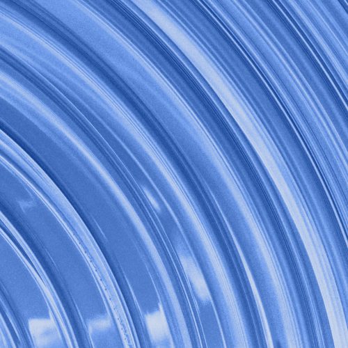
Curvilinear
News
Community
Videos
Join D
2
S
Contact Us
�
Menu
The Preferred GPU-Acceleration Partner for Semiconductor Manufacturing
Curvilinear Solutions in the Pixel Domain
Sorry, your browser doesn't support embedded videos.
Read More
Read More
Technologies
GPU Acceleration
Deep Learning
MB-MDP & MPC
Curvilinear
Products
CDP
TrueMask
®
ILT
TrueMask
®
MDP
TrueMask
®
DS
TrueMask
®
DLK
TrueModel
®
TrueMask
®
WPA
About D
2
S
About D
2
S
Timeline of D
2
S Technology Highlights
�
Technology
GPU Acceleration
Deep Learning
MB-MDP & MPC
Curvilinear
Products
CDP
TrueMask
®
ILT
TrueMask
®
MDP
TrueMask
®
DS
TrueMask
®
DLK
TrueModel
®
TrueMask
®
WPA
About D
2
S
About D
2
S
Timeline of D
2
S Technology Highlights
Information
News
Community
Videos
Join D
2
S
Contact Us
Read More
�
Menu
Technology
GPU Acceleration
Product
TrueMask
®
ILT
Learn More
Curvilinear
eBeam Community
Visit eBeam.org
Deep Learning Alliance
Visit CDLe.ai